ABSTRACT 1
1. THEORY
1.1 Time Delay Estimation (TDE)
1.2 Radar overview
1.3 Principle of Pulse Compression
1.4 Matched Filter
2. MATCHED FILTER DESIGN
3. IMPLEMENTATION AND TOOLS USED
3.1 Chip description
3.2 Tools Utilised
4. SIGNIFICANCE AND FUTURE WORK
References
Appendix A-Map Report 42
Appendix B-Pin Report 43
Appendix C-Post Layout Timing Report 45
Figure 2-1: Design Hierarchy
Figure 3-1: Pin Diagram of the chip
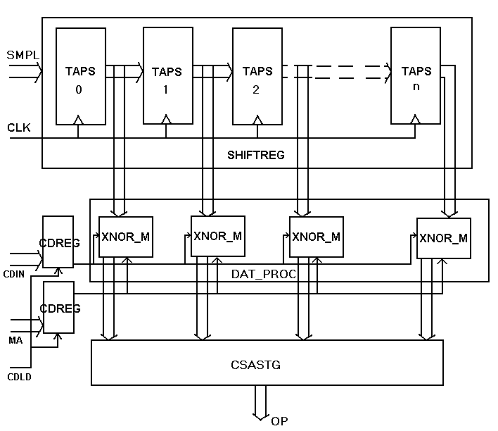
Figure 3-2: Internal structure of the chip
The choice for a radar signal has been governed by various factors including power considerations, maximum range and resolution distance. The search for a waveform that satisfies these criteria in an optimal fashion has always been on. Pulse compressed coding has emerged as one such solution. Pulse compressed code signals are detected on return with the help of matched filters. This project is an implementation of a matched filter stage for a pulse compressed and coded radar signal detector using Xilinx FPGAs.
Time delay estimation (TDE) or time of arrival (TOA) is a basic tool in statistical signal processing. Applications of TDE follow from the simple relationship given by
R= v t
R, is the distance of the object,
v, the velocity of the wavefield sent to the object, and
t, time taken for the wave to reach the object .
For example, in range measurements for radar or sonar, v is assumed known and the targets range is determined by measuring t , the time required for the transmitted signal to propagate to a target and be reflected back to point of transmission. Also for velocity measurements, like in biomedical or nuclear engineering applications, where R is assumed known and t the time required for a signal to travel the distance , R is measured.
In practice one seeks to measure the delay between two noisy versions of a signal. Unfortunately there is no single measurement procedure appropriate for all TDE scenarios. This fact, combined with practical importance of measuring time delay in so many different applications, is why TDE has received so much attention over the last three decades.
e(t) = x2(t) - x1(t-t)
An elementary form of radar consists of a transmitting antenna emitting electromagnetic radiation generated by an oscillator, a receiving antenna, and an energy detecting device or receiver. A portion of the transmitted signal is intercepted by a target, and reflected in all directions. The energy that is re-radiated in the direction of the radar is of prime importance. The receiving antenna collects the returned energy and delivers it to the receiver, where it is processed to detect the presence of a target and to determine its position and its relative velocity. The distance of the target is determined by measuring the time taken for the signal to travel to the target and back. The direction, or angular position, of the target may be determined by the direction of arrival of the reflected wave-front.
The most common radar waveform is a train of narrow rectangular shaped pulses modulating a sine wave carrier. The distance is measured as a function of the time taken by the transmitting pulse to travel to the target and back. Since electromagnetic waves travel at the velocity of light, the distance is given by
R = c T/2
R is the range of the target,
T is the time take by the Tx pulse to travel to target and return,
c is the velocity of the radar signal in space.
Pavg = Pp * duty ratio
= Pp * t / T
= Pp * t * F
Pp is the peak transmitted power,
t is the sub pulse width of the Transmitted wave,
F is the peak repetition frequency (PRF)
Hence the maximum detectable range can be improved by increasing Pp, t or F. Let us consider the three possibilities in detail.
Pulse compression involves the transmission of a long coded pulse and processing of the received echo to obtain a relatively narrow pulse. A long pulse may be obtained from a narrow pulse. Narrow pulses contain a large number of frequency components with a precise phase relationship between them if the relative pulses are changed by a phase distorting filter, the frequency components combine to produce a stretched or expanded pulse. The expanded pulse is then transmitted. The received echo is processed in the receiver by a compression filter. The compression filter readjusts the relative phases of the frequency components so that a narrow or compressed pulse is again produced.
An example of a pulse compression radar is phase coded pulse compression. In pulse coded waveform the long pulse is sub-divided into a number of shorter subplulses of equal duration. Each is then transmitted with a particular phase in accordance with a phase code (usually binary coding). Phase of the transmitted signal alternates between 0 & 180 degrees in accordance with the sequence of elements: 1s and 0s (+1s & -1s) in the phase code. The phase code used is generally a standard code, which has proved to provide the best resolution and least ambiguity in determining the target parameters. The codes used can be either Barker (which is given below) or some form of pseudo random code. The former is restricted to a maximum of 13 bits while the latter can be of any length. Commercial radars use codes of length nearly 50 to 60 bits.
| Code Length | Code Elements | Sidelobe level |
| 2 | 10, 11 | -6.0 |
| 3 | 110 | -9.5 |
| 4 | 1101,1110 | -12.0 |
| 5 | 11101 | -14.0 |
| 7 | 1110010 | -16.9 |
| 11 | 11100010010 | -20.8 |
| 13 | 1111100110101 | -22.3 |
R(t) = -T/2ò T/2 v1(t) v2(t + t) dt
lt T® µ
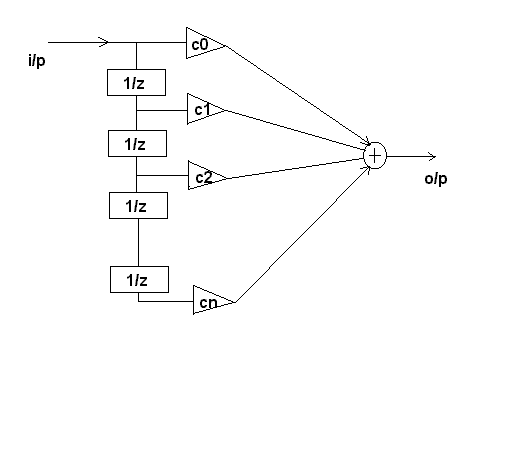
The phase coded received signal enters the taps one by one. The signal is unchanged of the coefficient of the tap is 1 and inverted in phase if it is -1. The coefficients of multiplication are the code in reverse form. The products are summed and the output obtained has maximum signal to noise ratio.
The matched filter used for time delay estimation is a generalized cross correlator. It is in the form of a simple FIR filter without feedforward or feedback as shown in the figure 1-2. It does the correlation of the samples and the code at each clock edge. This has to be done within 200ns which is the sub-pulse width of the radar signal.
Matched filter can be implemented as a software program or a hardware device. Software implementation has the advantage of early implementability. But in real time the embedded system executing the correlation will take more time for execution. This limits the performance of the radar signal processor for which this matched filter is a component. So our matched filter was designed as a single chip using Very high-speed integrated circuit Hardware Description Language [VHDL] and implemented on XILINX Field Programmable Gate Array [FPGA] XC4010PC84. FPGAs are a class of reconfigurable hardware devices generally used for prototyping Application Specific Integrated Circuits [ASICs] or to develop hardware with low Non-Recurring-Engineering [NRE] costs. These are the reasons for going in for FPGA implementation.
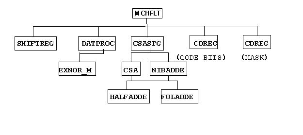
MACHFLT: This is the top-level entity where all the components are combined together. It consists of basically four components a shift register stage SHIFTREG, DATPROC, CSASTG, CDREG.
SHIFTREG: It is a twelve bits, sixteen stage register. i.e. it takes in 12 bits of data at each clock pulse and shifts it right by one stage on the next clock. It consists of sixteen such stages. This stage is used as the tap delays. This is designed as a behavioral model.
DATPROC: This does the processing of the outputs of the taps. It does the Multiplication of the samples with code-bits and masking the unused tap outputs.
CSASTG: This component is the adder stage, which adds all the sixteen, twelve bit numbers. Using carry propagate adders to add all the numbers will limit the speed. So the adder stage is implemented using carry-save adders. At the output of each adder a sum vector and a shifted carry vector is obtained. These are used as separate numbers in the next stage. All these are added as carry save adders. The final carry and sum vectors are added with a carry-propagate adder.
CDREG: These are 16-bit registers used for storing the code bits and masking bits.
The input for the implemented matched filter using 16 bit code is 12 bit digital samples from the Analog to Digital Converter. Each sample is shifted through a set of 16 stage 12 bit parallel register (output of one stage is given to the input of the next stage). Each bit in the pulse code is available in each register stage at any instant. These shift registers act as the taps in the block diagram. The output of the taps are multiplied by the code (+1s and -1s). As the numbers involved are large multiplying by a -1 is approximated to complementing of the 12 bit sample. This multiplication is done with the help of an array of 12 XNOR gates(on each for each bit of the sample. The output is determined by the code bit at that stage. If the code bit is 0 the samples are complemented(multiply by -1) and vice-versa. The output of each of these 16 XNOR arrays or multipliers have to be added at the next level to obtain the auto correlation function. The adder must add 16 numbers of 12 bit length. This is done with the help of a CSA adder. The final result is the auto correlation function at the sampled instant.
The project was implemented on a XC4010E having 10000 equivalent gates. The design consumed 9018 equivalent gates and utilised 388 out of 400 CLBs and 61 out of 61 IOBs.
The chip diagram of the implemented chip is as shown in Figure 3-1.
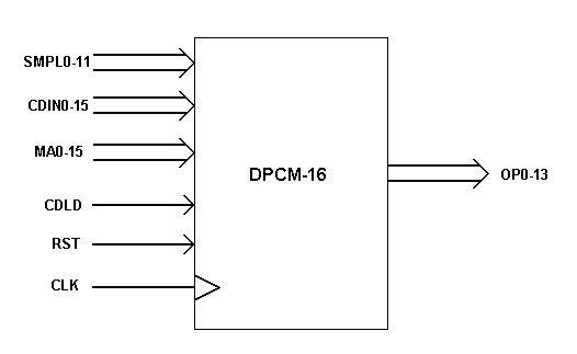
SMPL0-11: These are the 12-bit input samples to the chip. It enters the shiftregister[taps].
CDIN0-15: These are the pins using which the code is input to the chip.
MA0-15: These are the masking bits. Both mask and code bits are input to a parallel register.
CDLD: This is the enabling signal for the code and mask inputs.
RST: This is the system reset resets all the flops in the chip.
OP0-13: These are the output pins.
The internal structure of the chip is as shown in Figure 3-2.
Estimated performance that could be achieved using this matched filter is a resolution capacity of 60m. As given in the theory, the maximum Barker code available is 13-bit wide. This matched filter supports all the Barker codes. The features included in the chip like masking and code load makes the filter programmable for different codes of different widths.
Range of the radar can be further increased without forgoing the resolution capacity by using longer codes with the same sub-pulse width. Such codes established for radar TDEs are Pseudo-Random codes typically of 54-bits wide. This provides scope for future improvement upon this project.
1. M.Skolnik, "Introduction to Radar Systems." pub.-McGraw Hill, 2nd edition, 1980.
2. "Special issue on Time delay estimation." IEEE Transactions on ASSP, Vol ASSP-29,1981.
3. John Villasenor and Brad Hutchings, "The Flexibility Of Configurable Computing." IEEE Signal Processing, vol.15, no. 5, Sept 1998.
4. Mazor & Langstrat, "A guide to VHDL." pub.-Kluwer Academic Publisher, 1st edition, 1995.
5. Douglas Perry, "VHDL." pub.-McGraw Hill, 2nd edition, 1995.
MAP REPORT
Design Information
------------------
Target Device : x4010e
Target Package : pc84
Target Speed : -1
Mapper Version : xc4000e -- M1.5.19
Design Summary
--------------
Number of errors: 0
Number of warnings: 1
Number of CLBs: 388 out of 400 97%
CLB Flip Flops: 224
4 input LUTs: 629
3 input LUTs: 216
Number of bonded IOBs: 61 out of 61 100%
IOB Flops: 0
IOB Latches: 0
Number of clock IOB pads: 2 out of 8 25%
Number of primary CLKs: 2 out of 4 50%
13 unrelated functions packed into 13 CLBs.
(3% of the CLBs used are affected.)
Total equivalent gate count for design: 6090
Appendix B
PIN REPORT
Pinout by Pin Name:
+--------------------------------------------------------------------------------------------
| Pin Name | Direction|Pin Number|
+--------------------------------------------------------------------------------------------
| CDIN<0> | INPUT | P18 |
| CDIN<10> | INPUT | P48 |
| CDIN<11> | INPUT | P51 |
| CDIN<12> | INPUT | P39 |
| CDIN<13> | INPUT | P38 |
| CDIN<14> | INPUT | P68 |
| CDIN<15> | INPUT | P67 |
| CDIN<1> | INPUT | P19 |
| CDIN<2> | INPUT | P46 |
| CDIN<3> | INPUT | P47 |
| CDIN<4> | INPUT | P28 |
| CDIN<5> | INPUT | P26 |
| CDIN<6> | INPUT | P10 |
| CDIN<7> | INPUT | P9 |
| CDIN<8> | INPUT | P81 |
| CDIN<9> | INPUT | P79 |
| CDLD | INPUT | P13 |
| CLK | INPUT | P35 |
| MA<0> | INPUT | P14 |
| MA<10> | INPUT | P69 |
| MA<11> | INPUT | P71 |
| MA<12> | INPUT | P61 |
| MA<13> | INPUT | P62 |
| MA<14> | INPUT | P59 |
| MA<15> | INPUT | P66 |
| MA<1> | INPUT | P16 |
| MA<2> | INPUT | P44 |
| MA<3> | INPUT | P45 |
| MA<4> | INPUT | P27 |
| MA<5> | INPUT | P29 |
| MA<6> | INPUT | P8 |
| MA<7> | INPUT | P7 |
| MA<8> | INPUT | P83 |
| MA<9> | INPUT | P82 |
| OP<0> | OUTPUT | P65 |
| OP<10> | OUTPUT| P58 |
| OP<11> | OUTPUT | P57 |
| OP<12> | OUTPUT | P49 |
| OP<13> | OUTPUT | P50 |
| OP<1> | OUTPUT | P23 |
| OP<2> | OUTPUT | P20 |
| OP<3> | OUTPUT | P60 |
| OP<4> | OUTPUT | P84 |
| OP<5> | OUTPUT | P80 |
| OP<6> | OUTPUT | P78 |
| OP<7> | OUTPUT | P70 |
| OP<8> | OUTPUT | P72 |
| OP<9> | OUTPUT | P56 |
| RST | INPUT | P77 |
| SMPL<0> | INPUT | P24 |
| SMPL<10> | INPUT | P36 |
| SMPL<11> | INPUT | P37 |
| SMPL<1> | INPUT | P25 |
| SMPL<2> | INPUT | P17 |
| SMPL<3> | INPUT | P15 |
| SMPL<4> | INPUT | P5 |
| SMPL<5> | INPUT | P6 |
| SMPL<6> | INPUT | P4 |
| SMPL<7> | INPUT | P3 |
| SMPL<8> | INPUT | P40 |
| SMPL<9> | INPUT | P41 |
+------------------------------------------------------------------------------------------
| Dedicated or Special Pin Name | Pin Number |
+------------------------------------------------------------------------------------------
| /PROG | P55 |
| CCLK | P73 |
| DONE | P53 |
| GND | P21 |
| GND | P64 |
| GND | P43 |
| GND | P52 |
| GND | P12 |
| GND | P31 |
| GND | P1 |
| GND | P76 |
| M0 | P32 |
| M1 | P30 |
| M2 | P34 |
| TDO | P75 |
| VCC | P63 |
| VCC | P2 |
| VCC | P22 |
| VCC | P54 |
| VCC | P74 |
| VCC | P33 |
| VCC | P11 |
| VCC | P42 |
+--------------------------------------------------------------------+--------------+
Appendix C
POST LAYOUT TIMING REPORT
Timing summary:
---------------
Timing errors: 0 Score: 0
Constraints cover 186795 paths, 805 nets, and 2159 connections (100.0% coverage)
Design statistics:
Minimum period:14.607ns (Maximum freq:68.460MHz)
Maximum combinational path delay: 81.383ns
Maximum net delay: 13.628ns
---------------------------------------------------------